- 您现在的位置:买卖IC网 > Sheet目录2000 > IDT5V49EE902NLGI (IDT, Integrated Device Technology Inc)IC CLOCK GEN PLL 500MHZ 32VFQFPN
IDT5V49EE902
EEPROM PROGRAMMABLE CLOCK GENERATOR
CLOCK SYNTHESIZER
IDT EEPROM PROGRAMMABLE CLOCK GENERATOR
3
IDT5V49EE902
REV P 092412
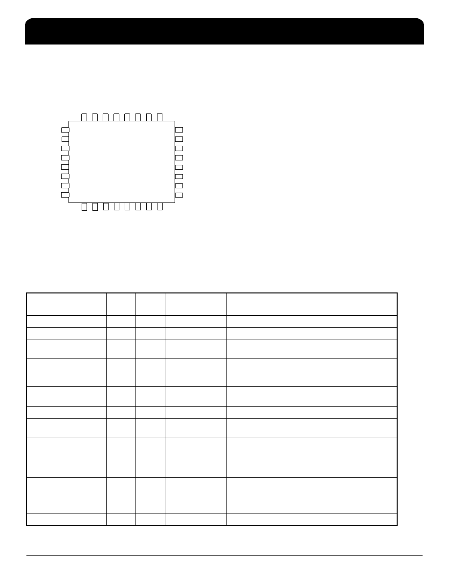
PIN CONFIGURATION
.
Pin Descriptions
32 pin VFQFPN
(Top View)
16
VDDO
5
15
OU
T5b
11
OU
T
4
b
14
OU
T5
13
GN
D
12
VDDO
4
10
OU
T
4
9
VDDO
1
17
GND
18
SDAT
20
CLKSEL
21
AVDD
22
GND
OUT6
23
24
OUT3
SCLK
19
25
VDDO3
SE
L
2
26
27
SE
L
1
28
SE
L
0
31
GND
30
OU
T0
32
VD
D
29
S
D
/OE
1
VDD
2
XOUT
4
VDDx
3
XIN/REF
5
CLKIN
GND
6
7
OUT1
OUT2
8
Pin Name
NL32
Pin#
I/O
Pin Type
Pin Description
CLKIN
5
I
LVTTL
Input clock. Weak internal pull down resistor.
XOUT
2
O
LVTTL
CRYSTAL_OUT -- Reference crystal feedback.
XIN / REF
3
I
LVTTL
CRYSTAL_IN -- Reference crystal input or external
reference clock input.
SDAT
18
I/O
Open Drain
Bidirectional I2C data. An external pull-up resistor is
required. See I2C specification for pull-up value
recommendation.
SCLK
19
I
LVTTL
I2C clock. An external pull-up resistor is required. See
I2C specification for pull-up value recommendation.
CLKSEL
20
I
LVTTL
Input clock selector. Weak internal pull down resistor.
SEL2
26
I
LVTTL
Configuration select pin. Weak internal pull down
resistor.
SEL1
27
I
LVTTL
Configuration select pin. Weak internal pull down
resistor.
SEL0
28
I
LVTTL
Configuration select pin. Weak internal pull down
resistor.
SD/OE
29
I
LVTTL
Enables/disables the outputs or powers down the chip.
The SP bit (0x02) controls the polarity of the signal to be
either active HIGH or LOW. (Default is active LOW.)
Weak internal pull down resistor.
OUT0
30
O
LVTTL
Configurable clock output 0. 3.3V LVTTL levels.
发布紧急采购,3分钟左右您将得到回复。
相关PDF资料
IDT5V49EE904NLGI8
IC PLL CLK GEN 200MHZ 32VFQFN
IDT821024PPG
IC PCM CODEC QUAD NONPROG 44TQFP
IDT821034DNG
IC PCM CODEC QUAD MPI 52-PQFP
IDT821054PQF
IC PCM CODEC QUAD MPI 64-PQFP
IDT82V3001APVG8
IC PLL WAN W/SGL REF INP 56-SSOP
IDT82V3010PVG
IC PLL WAN 51/E1/OC3 DUAL 56SSOP
IDT82V3011PVG
IC PLL WAN T1/E1/OC3 SGL 56-SSOP
IDT82V3012PVG8
IC PLL WAN T1/E1/OC3 DUAL 56SSOP
相关代理商/技术参数
IDT5V49EE902NLGI8
制造商:Integrated Device Technology Inc 功能描述:IC CLK GEN EEPROM PROGR 32QFN
IDT5V49EE903NLGI
制造商:Integrated Device Technology Inc 功能描述:IC CLOCK GENERATOR
IDT5V49EE903NLGI8
制造商:Integrated Device Technology Inc 功能描述:IC CLK GEN EEPROM PROGR 32QFN
IDT5V49EE903PGGI
制造商:Integrated Device Technology Inc 功能描述:IC CLOCK GENERATOR
IDT5V49EE903PGGI8
制造商:Integrated Device Technology Inc 功能描述:IC CLK GEN EEPROM PROGR 28TSSOP
IDT5V49EE904NLGI
功能描述:IC PLL CLK GEN 200MHZ 32VFQFN RoHS:是 类别:集成电路 (IC) >> 时钟/计时 - 时钟发生器,PLL,频率合成器 系列:VersaClock™ III 标准包装:2,000 系列:- 类型:PLL 频率合成器 PLL:是 输入:晶体 输出:时钟 电路数:1 比率 - 输入:输出:1:1 差分 - 输入:输出:无/无 频率 - 最大:1GHz 除法器/乘法器:是/无 电源电压:4.5 V ~ 5.5 V 工作温度:-20°C ~ 85°C 安装类型:表面贴装 封装/外壳:16-LSSOP(0.175",4.40mm 宽) 供应商设备封装:16-SSOP 包装:带卷 (TR) 其它名称:NJW1504V-TE1-NDNJW1504V-TE1TR
IDT5V49EE904NLGI8
功能描述:IC PLL CLK GEN 200MHZ 32VFQFN RoHS:是 类别:集成电路 (IC) >> 时钟/计时 - 时钟发生器,PLL,频率合成器 系列:VersaClock™ III 标准包装:1,000 系列:- 类型:时钟/频率合成器,扇出分配 PLL:- 输入:- 输出:- 电路数:- 比率 - 输入:输出:- 差分 - 输入:输出:- 频率 - 最大:- 除法器/乘法器:- 电源电压:- 工作温度:- 安装类型:表面贴装 封装/外壳:56-VFQFN 裸露焊盘 供应商设备封装:56-VFQFP-EP(8x8) 包装:带卷 (TR) 其它名称:844S012AKI-01LFT
IDT5V50009DCG
功能描述:IC PC CLOCK 8-SOIC RoHS:是 类别:集成电路 (IC) >> 时钟/计时 - 时钟发生器,PLL,频率合成器 系列:- 标准包装:39 系列:- 类型:* PLL:带旁路 输入:时钟 输出:时钟 电路数:1 比率 - 输入:输出:1:10 差分 - 输入:输出:是/是 频率 - 最大:170MHz 除法器/乘法器:无/无 电源电压:2.375 V ~ 3.465 V 工作温度:0°C ~ 70°C 安装类型:* 封装/外壳:* 供应商设备封装:* 包装:*